Purdue-Argonne collaboration developing faster, non-destructive technique for detecting problems in semiconductors

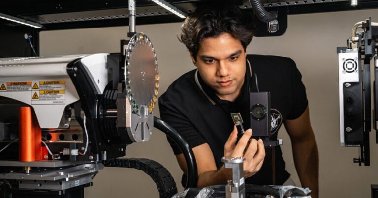
Materials engineering doctoral student Sidhaant Vasudeva places a semiconductor chip for imaging on an X-ray microscope at Purdue University’s Flex Lab. Nikhilesh Chawla, Ransburg professor of materials engineering at Purdue and an expert in four-dimensional materials science, is working with Argonne National Laboratory to better detect defects in semiconductor chips. (Photo by Purdue University/Kelsey Lefever)
WEST LAFAYETTE, Ind. — A defect in a semiconductor chip can be smaller than a human hair, but can create big problems in your daily life, from crippling the steering of your car to making your laptop more vulnerable to hackers.
Nikhilesh ChawlaA Purdue University engineer, works with academic colleagues and scientists at the U.S. Department of Energy (DOE) Argonne National Laboratory on high-resolution imaging to better spot defects and speed up the existing inspection process during chip manufacturing.
“Studying semiconductor defects and being able to detect them quickly so we can help the industry is a very important topic,” said Chawla, the Purdue professor in Ransburg. Materials engineering. “We hope to speed up the whole process by using new imaging techniques and faster algorithms.”
The research examines several aspects of defects, including how they form and whether a particular phase of semiconductor packaging is more susceptible to defects during the manufacturing process. The packaging refers to several electrically connected chips. Advanced packaging aims to revolutionize packaging by enabling complex functionality while reducing costs.
Chawla said the work is divided into three areas, starting with high-resolution imaging which must be able to see the smallest possible defects. To do this, he works with X-ray imaging and X-ray tomography at Advanced Photon Source, a DOE Office of Science user facility at Argonne, to create a 3D microstructure of the chip. Once defects are located, the technique works backward through the process to determine where defects may have initially formed.
The second stage uses artificial intelligence to ensure that the detection technique is faster and smarter with more efficient algorithms to process imaging data and ensure automatic detection of defects so that the manufacturing process is not hampered.
“The third part is understanding which category of defects is going to cause problems for the chip in the field,” Chawla said. “By understanding which ones are actually going to cause problems in the device, we can detect them in the manufacturing cycle and prevent failures from happening to the customer.”

The project team also includes Purdue’s Charles Bouman, Showalter Professor of Electrical and Computer Engineering and Biomedical Engineering; Greg Buzzard, mathematics teacher; and Hany Abdel-Khalik, professor of nuclear engineering, as well as Francesco de Carlo of Argonne, Erdogan Madenci of the University of Arizona and Martin Gall of GlobalFoundries.
Purdue’s national leadership in microelectronics and semiconductors is the cornerstone of Purdue calculates – a global initiative that spans IT departments, physical AI, quantum science and semiconductor innovation. The university’s cutting-edge research, transformational investments in infrastructure and workforce development programs set a national benchmark for excellence and spearhead a growing semiconductor cluster in West Lafayette.
Chawla’s research with Argonne is being conducted as part of the National Science Foundationof the Future of Semiconductors program. Chawla said he expects the work to be published as soon as the end of the year.
For industry, this technique could offer a new way to deal with semiconductor chip problems.
“The semiconductor industry is used to taking a faulty component and cutting it up, which is very laborious and time-consuming, and on top of that you lose the part as well,” Chawla said. “Through a non-destructive imaging technique, we hope to be able to obtain snapshots of the chip structure during the manufacturing process, so you know the state of a component.”
Data from this technical research could lead to future probabilistic uses, such as using imaging data to help determine the time frame in which a fault could cause a device such as a cell phone to fail.
About Purdue University
Purdue University is a public research university leading in large-scale excellence. Ranked among the top 10 public universities in the United States, Purdue discovers, disseminates and deploys knowledge with unparalleled quality and scale. More than 106,000 students study at Purdue across multiple campuses, locations and modalities, including more than 57,000 on our main campuses in West Lafayette and Indianapolis. Committed to affordability and accessibility, Purdue’s main campus has frozen tuition 14 years in a row. Learn how Purdue never stops in its persistent pursuit of the next giant leap, including its integrated and comprehensive urban expansion of Indianapolis; the Mitch Daniels School of Business; Purdue calculates; and the One Health initiative — to https://www.purdue.edu/president/strategic-initiatives
